- 您现在的位置:买卖IC网 > Sheet目录983 > HI5714EVAL (Intersil)EVALUATION PLATFORM HI5714
�� �
�
�Application� Note� 9517�
�Table� 1� lists� the� operating� conditions� for� the� power� supplies.�
�TABLE� 1.� POWER� SUPPLIES�
�Input� Clock� Driver� and� Timing�
�The� clock� input� to� the� HI5174� evaluation� board� should� be�
�POWER�
�SUPPLY�
�+5VA�
�-5.2VA�
�+5VD�
�+12V�
�-12V�
�MIN�
�+4.75V�
�-5.3V�
�+4.75V�
�+10V�
�-10V�
�TYP�
�+5.0V�
�-5.2V�
�+5.0V�
�+12V�
�-12V�
�MAX�
�+5.25V�
�-5.0V�
�+5.25V�
�+15V�
�-15V�
�CURRENT�
�TYP�
�25mA�
�-120mA�
�136mA�
�25mA�
�-20mA�
�driven� with� a� standard� TTL� level� signal.� U4� (75F04)� will�
�buffer� the� clock� input� and� drive� the� HI5714� as� well� as� the� 26�
�pin� connector.� For� optimum� performance� of� the� HI5714� the�
�duty� cycle� of� the� clock� should� be� kept� at� 50%� ±� 10%.� U5� and�
�U6� (74F541)� will� buffer� the� output� bits� and� keep� the� power�
�transients� caused� by� charging� a� large� bus� capacitance� off�
�the� supplies� to� the� ADC.�
�As� with� any� high� speed� ADC,� clock� jitter� (in� this� case�
�external)� must� be� accounted� for.� Clock� jitter� will� cause� the�
�Reference� Circuit�
�For� the� following� discussion,� refer� to� the� board� schematic�
�and� the� board� layout� drawing.�
�The� HI5714� requires� two� reference� voltages:� V� RT� and� V� RB� .�
�The� external� voltage� reference� generator� on� the� evaluation�
�converter� to� sample� at� a� nonuniform� rate,� thus� having� the�
�effect� of� distorting� the� digital� representation� and� raise� the�
�noise� floor.� For� this� reason,� users� should� take� care� to�
�provide� as� uniform� a� clock� signal� as� possible� to� assure�
�optimal� performance.�
�TABLE� 2.� TIMING� SPECIFICATIONS�
�board� is� used� to� generate� a� V� RT� of� about� 3.6V� and� a� V� RB� of�
�about� 1.3V.� The� ICL8069� reference� diode� generates� a� 1.2V�
�voltage� that� is� gained� up� by� two� op� amps� to� the� reference�
�voltages� V� RT� and� V� RT� for� the� ADC.� V� RT� should� be� kept� in�
�the� range� of� 3.5V� to� 3.9V.� P1� is� adjusted� at� the� factory� for� a�
�V� RB� of� 1.3V� ±� 2mV.�
�Analog� Input�
�PARAMETER�
�t� OD�
�t� PD1�
�t� PD2�
�t� PD3�
�DESCRIPTION�
�HI5714� Data� Delay�
�74F04� Prop� Delay�
�74F04� Prop� Delay�
�74F541� Prop� Delay�
�MIN�
�-�
�2.4ns�
�2.4ns�
�2.1ns�
�TYP�
�10ns�
�-�
�-�
�-�
�MAX�
�13ns�
�8.5ns�
�8.5ns�
�7.5ns�
�The� analog� input� to� the� HI5174� can� be� configured� in� various�
�ways� depending� on� the� input� signal� and� the� required� level� of�
�performance.� A� signal� voltage� with� a� maximum� span� of� V� RT� to�
�V� RB� can� be� AC� coupled� to� the� HI5714� through� the� V� IN2� BNC�
�and� applied� to� the� ADC� by� installing� jumper� JP2.� P4� would� be�
�adjusted� to� center� the� signal� in� the� range� of� the� HI5714.� This�
�may� or� may� not� be� adequate� depending� on� the� type� of� input�
�signal.�
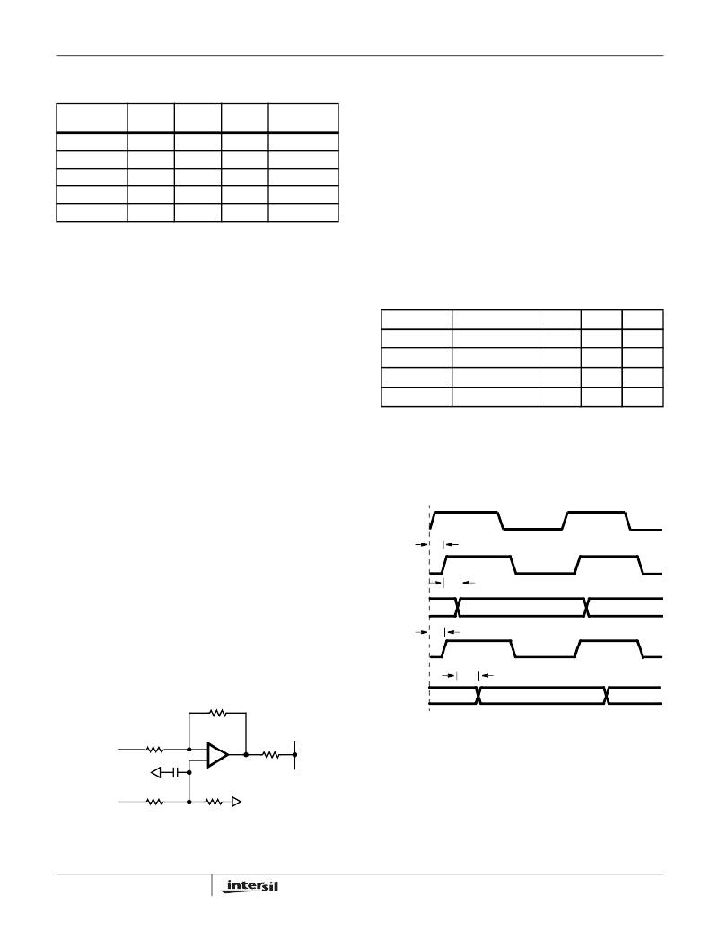
�Figure� 6� shows� the� timing� for� the� evaluation� board.� The� data�
�corresponding� to� a� particular� sample� will� be� available� at� the�
�output� of� the� HI5714� after� the� required� data� latency� (1� cycle)�
�plus� an� output� delay.� Table� 2� lists� the� values� that� can� be�
�expected� for� the� various� timing� delays.� Refer� to� the�
�datasheet� for� additional� timing� information.�
�CLK1�
�INPUT�
�An� HA5020� buffer� (as� shown� in� Figure� 5)� is� also� provided�
�that� can� be� used� to� drive� the� part� by� inserting� JP1.� The� gain�
�of� the� circuit� can� be� calculated� from:�
�HI5714�
�CLOCK�
�t� PD1�
�V� OUT� =� –� ?� -------� ?� V� IN� +� ?� 1� +� -------� ?� ?� ---------------------� ?� V� OFFSET�
�?� R� 9� ?� ?� R� 9� ?� ?� R� 1� ?�
�?� R� 7� ?� ?� R� 7� ?� ?� R� 1� +� R� 2� ?�
�The� combination� of� the� buffer� and� the� external� reference� will�
�give� the� best� performance� for� the� HI5714� and� allow� the� most�
�INPUT�
�HI5714�
�DATA0-7�
�OUTPUT�
�t� OD�
�t� PD2�
�DATA�
�DATA�
�flexibility� when� dealing� with� various� types� of� input� signals.� If�
�an� application� is� extremely� cost� sensitive� then� the� internal�
�bias� generators� along� with� the� AC� coupled� version� of� the�
�CLK� OUT�
�(74ACT04)�
�t� PD3�
�input� circuit� can� be� used.�
�DOUT0-7�
�(74ACT541)�
�DATA�
�DATA�
�V� IN�
�R� 7�
�R� 9�
�-�
�+�
�R� 2�
�V� IN�
�FIGURE� 6.� INPUT-TO-OUTPUT� TIMING�
�DAC� Setup�
�V� OFFSET�
�0.1� μ� F�
�R� 2� R� 1�
�FIGURE� 5.� MODIFIED� BUFFER�
�The� HI5721� is� used� as� a� reconstruct� DAC� to� allow� the� user�
�to� easily� view� the� performance� of� the� HI5714.� The� HI5721� is�
�a� TTL,� 10-bit,� 125MHz� DAC.�
�The� internal� reference� in� the� HI5721� is� a� -1.25V� (typical)�
�bandgap� voltage� reference� with� a� 100� μ� V/� o� C� temperature�
�drift.� The� internal� reference� should� be� buffered� by� the�
�3�
�发布紧急采购,3分钟左右您将得到回复。
相关PDF资料
HI5728EVAL1
EVALUATION PLATFORM TQFPHI5728
HI5731-EVS
EVALUATION PLATFORM SOIC HI5731
HI5741-EVS
EVALUATION PLATFORM HI5741
HI5760EVAL1
EVALUATION PLATFORM SOIC HI5760
HI5762EVAL2
EVALUATION MOD FOR HI5762 AMP
HI5767EVAL1
EVALUATION PLATFORM HI5767
HI5767EVAL2
EVALUATION PLATFORM HI5767
HI5805EVAL1
EVALUATION PLATFORM HI5805
相关代理商/技术参数
HI5721
制造商:INTERSIL 制造商全称:Intersil Corporation 功能描述:10-Bit, 125 MSPS, High Speed D/A Converter
HI5721 WAF
制造商:Harris Corporation 功能描述:
HI5721_03
制造商:INTERSIL 制造商全称:Intersil Corporation 功能描述:10-Bit, 125MSPS, High Speed D/A Converter
HI5721BIB
制造商:Rochester Electronics LLC 功能描述: 制造商:Harris Corporation 功能描述: 制造商:Intersil Corporation 功能描述:
HI5721BIBS2503
制造商:Rochester Electronics LLC 功能描述:- Bulk
HI5721BIB-T
制造商:Rochester Electronics LLC 功能描述:HI5721BIB IN TAPE & REEL - Bulk
HI5721BIB-TS5001
制造商:Rochester Electronics LLC 功能描述:- Bulk
HI5721BIP
制造商:Rochester Electronics LLC 功能描述:28 PDIP INDTEMP D/A 10 BIT 125 MHZ -5.2V - Bulk